Sciences & Technology
Diamonds reveal neural secrets
A new way to measure the flow of electricity in a diamond electrical device reveals an unexpected phenomenon reminiscent of lightning in slow motion
Published 3 September 2024
Diamond is in many ways the ultimate material.
Besides its enduring aesthetic value, diamond is also a highly versatile industrial material.
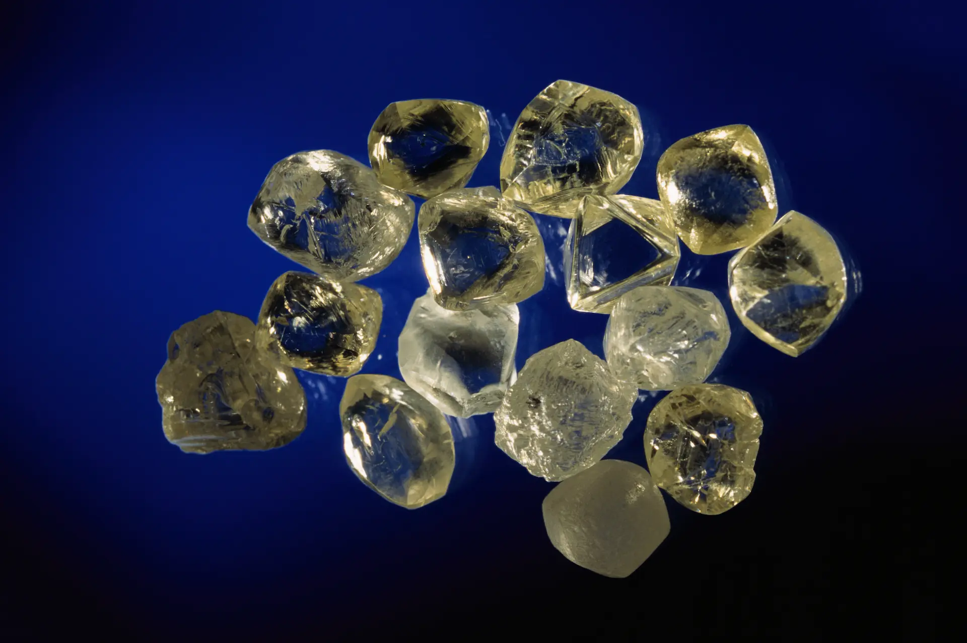
While its claim as the hardest substance known to science has been usurped by ultra-rare minerals and newly developed synthetic materials, it still sits on the top of many rankings of material properties.
Diamond’s ability to conduct heat (its ‘thermal conductivity’) is unparalleled, and it also forms an ideal host environment for quantum bits (qubits) that are currently revolutionising magnetic field sensors and could one day make possible room-temperature quantum computing.
What is perhaps less widely known is that diamond is also the ultimate material for high-power electronics: the circuit elements critical in power plants, electrical distribution substations, electric cars and other emerging technologies.
At least theoretically.

Sciences & Technology
Diamonds reveal neural secrets
None of these technologies currently use diamond, and the vast majority use silicon, which needs to be kept cool and has limits on the voltages it can work at.
Something like 10 per cent of electrical power that is generated is wasted due to silicon’s limitations, and diamond could reduce these losses by 75 per cent. So why aren’t we driving electric cars packed with diamond power electronics?
Well, because diamond is hard! It’s hard to fabricate, hard to connect to metals, hard to make in large sizes and hard to engineer with the right impurities to tailor its electrical properties – all the things needed for scalable production of electronic components.
We also don’t yet fully understand how charges flow inside diamond, and how unavoidable impurities and defects affect these electrical properties.
In a recent study with colleagues from the University of Melbourne, RMIT University and the City College of New York, we sought to combine electrical measurements of a diamond optoelectronic device with 3D optical microscopy.
Our motivation was to understand several curious findings that others have reported when these two techniques – electrical measurements and optical microscopy – were used independently.
By combining them, we were able to see in striking three-dimensional detail for the first time what happens when charges enter and move through a diamond electronic device.
To do this we used impurities in the diamond crystal lattice that are formed from nitrogen atoms that sit next to a gap in the lattice – called nitrogen-vacancy or NV centres.

Sciences & Technology
Spinning diamonds for quantum precision
These NV centres are well-known as sensors and can act as qubits in quantum computing.
NV centres can be either neutral or negatively charged, and we can detect charges flowing in the diamond by monitoring the electric charge of these defects.
In our microscope, neutral NVs appear slightly more orange than negative NV centres, so we can create an image of where a current has flowed.
Our experiment consists of a diamond with many NV centres coated with two metallic electrodes inside an optical microscope.
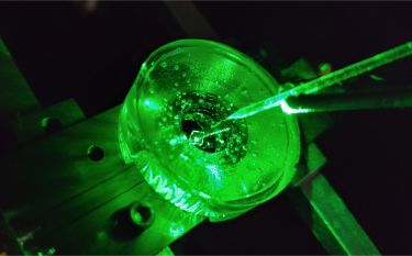
We use a green laser to generate an electric current in the diamond (similar to the process that turns light into electricity in solar cells) and then observe and record where that current flows.
Our technique maps out the full 3D structure of charge generation and flow over time.
What we saw was unexpected.
Current appears to flow from one side of the device to the other in thin, streamer-like filaments that start (nucleate) from specific points along the metal electrodes.
It is reminiscent of a lightning strike.
You may have heard that lightning comes from the ground and not the clouds. What happens is, immediately before a lightning strike an invisible darting channel of ionised gas called a stepped leader descends from the cloud to the ground.
This leader is attracted to features on the ground, such as tall trees or lighting rods on buildings.
The channel this leader leaves in the air presents a highly conducting path for the return stroke of visible lightning that then shoots up from the ground, creating a brilliant flash of forking, zigzagging light.

Sciences & Technology
Using quantum computing to protect AI from attack
Real lightning is thousands of amperes of current flowing in microseconds (millionths of a second), but similar principles underly the process occurring in our diamond, except it is measured in picoamps (one-trillionth of an amp) and over whole seconds.
In our diamond circuit, the electrons (the invisible ‘leader’) are drawn towards specific features on the metal-to-diamond connection (the ‘ground’).
As the electrons flow they create filament-like channels of increased conductivity behind them that the positive charge flows along in the ‘return stroke’ that we capture through our microscope.
Why do the electrons flow in filaments? We just don’t know – yet.

We think these specific ‘ground’ features on the electrode – analogous to the trees and skyscrapers that attract lightning – are in fact points where the electric contact with the diamond is better than other points.
We can use our technique to precisely locate these focal points, making this a powerful diagnostic tool that can shed light on the problem of creating good metal-to-diamond connections in electronic devices.
Through this study, we also showed that we can engineer the charge states of NV centres in the diamond to change how current flows.
We essentially draw patterns inside the diamond with lasers, ‘charging’ up the NV centres and other impurities, and creating a kind of circuit. This is a potential building block for creating optically reconfigurable diamond electronic devices.

Sciences & Technology
Looking inside a pigeon’s ear using quantum technology
Our work cracks open a whole new arena of research around controlling charge transport in diamonds and then imaging the results. This is important to both emerging high-power electronics and quantum technology.
We can also apply our technique to other materials far more advanced in their electronics applications, like silicon carbide, which is already powering newer generations of electric vehicles.
It will hopefully lead to improvements in interfacing electronics with quantum materials and in building room-temperature quantum computers using diamond.
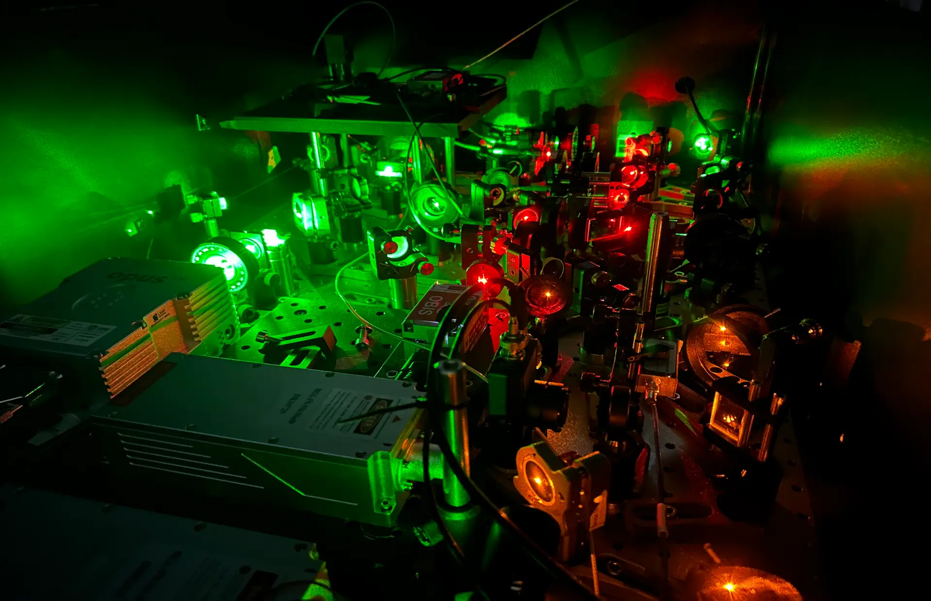
The banner image shows the array of lasers that control the charge of NV centres in the diamond and image where current flows. Green lasers are used for charge control, while orange and red lasers allow for imaging in three dimensions.