Sciences & Technology
Machine learning to scale up the quantum computer

A new material for nanowires, designed by computer simulations, paves the way for a new era of photonic and quantum electronic technologies, consuming less energy and reducing operating costs
Published 15 October 2020
Electronic and optical systems are integral parts of daily life, from simple household appliances like lights and television screens, to communication, computing and medical devices.
The quest for compact and cost-effective devices has been a key driving force behind the remarkable innovations in the last few decades.

Everyday users gauge the efficiency of optoelectronic devices (light harvesting and emitting technologies) like LED traffic lights and solar panels on their throughput, speed, cost or reliability.

Sciences & Technology
Machine learning to scale up the quantum computer
But at a fundamental level, it’s the nanomaterials and nanostructures that dictate the efficiency and the associated cost. So, breakthroughs in nanomaterials could bring transformative impact in nanoscale devices and may lead to a new era of superior technologies.
Our recent research published in Nanoscale journal applied state-of-the-art theoretical simulation tools to investigate the electronic and optical properties of nanowires made up of an emerging nanomaterial which may pave the way for new energy efficient nanodevices.
Nanowires are the long cylinders or rods which can be constructed from various semiconductor materials, these are materials with properties somewhere between those that conduct electricity and those that insulate.
Semiconductor materials include silicon or can be from a combination of other elements like gallium and arsenide (GaAs).

Nanowires are highly versatile nanostructures, which have found applications in many areas including light emission or sensing, medical devices, lasers, catalysis and transistors among others.

Sciences & Technology
Grasping the ‘spooky’ in Quantum physics
Typically nanowires are fabricated with large length to diameter ratios, varying from five to 100 or more. By varying nanowire size, shape or chemical compositions, we can achieve exquisite control over their optoelectronic properties – that is, how they interact with light.
Another sub-class of nanowires is known as core-shell nanowire. This is where nanowires are made up of two different materials, with one material surrounding the other material in the form of two concentric cylinders – the core and the shell.
Core-shell nanowires provide an additional mechanism for fine tuning their optoelectronic properties by varying relative chemical composition or diameters of the core and shell regions.
One of the most popular class of nanowire materials is a combination of periodic table group III element gallium and group V element arsenide forming a semiconductor material, Gallium Arsenide (GaAs).
The GaAs material offers promising light emission or absorption properties due to the associated direct band-gap. This is the amount of energy associated with the light absorbed or emitted from a material.
In the last few years, GaAs- based nanowires have been used in solar cells, lasers, light emitting diodes and transistors.
Despite promising optoelectronic characteristics, GaAs-based photonic devices suffer from high internal losses which generate heat.

Sciences & Technology
What could Australia’s clean energy future look like?
In fact, it is estimated that approximately 80 per cent of electrical power is wasted in a telecommunication wavelength laser device as heat. As a result, most systems require thermo-electric coolers and an air-conditioned environment, which further increases the energy budget by orders of magnitude.
To circumvent this problem, our latest research investigated a new material system – Gallium Bismuth Arsenide (GaBiAs) for the design of core-shell nanowires.
GaBiAs material is formed by adding dilute amounts of bismuth (Bi atoms, another group V element) in the GaAs material.
In the past, the addition of Bi in GaAs modifies the energy levels of the material in a way that the internal loss mechanisms are suppressed, leading to a significantly improved temperature sensitivity.
However, the incorporation of GaBiAs material in nanowire devices and its impact on optoelectronic properties was still not well understood until now.
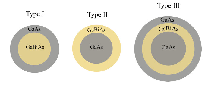
To thoroughly investigate the role of GaBiAs in core-shell nanowires, our recent studies investigated three different types of nanowires (Figure 1), now published in a pair of Nanoscale journal articles in 2019 and 2020.

Sciences & Technology
Wearable devices that use human energy
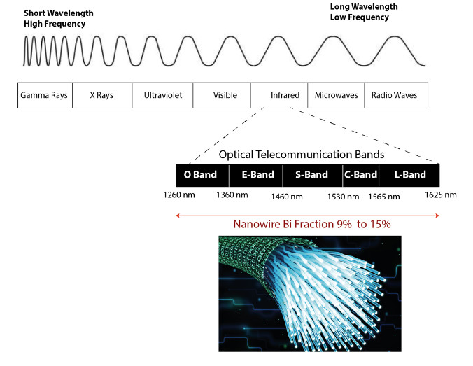
The work demonstrated that the incorporation of bismuth in GaAs nanowires provides a control to vary the band-gap energy over a large range that includes the wavelength requirements for devices used in optical communication systems (Figure 2), making them suitable for multi-billion dollar photonic device industry.
The studies also revealed that by merely changing the relative diameters of core and shell regions, the nanowires can be designed for strong light interaction (emission or absorption) suitable for devices like LEDs and lasers, or for large light to electric charge conversion suitable for solar cells.
The research concluded that nanowires made up of GaBiAs semiconductors may lead to a new generation of ‘green’ photonic devices which will consume drastically less energy – significantly reducing their operational cost to provide a sustainable and environmentally friendly solution.
Bismuth atoms are quite different from arsenic atoms, so replacing As with Bi in GaAs introduces unique changes in the electronic properties of the material.
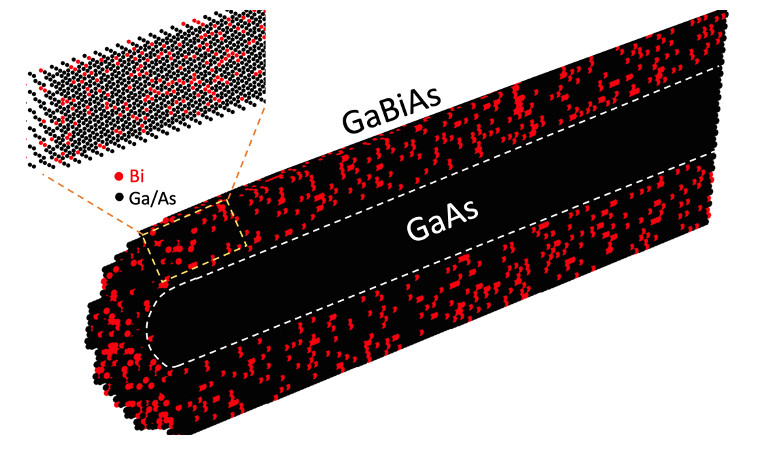
In order to capture the realistic impact of Bi in GaAs, we constructred nanowires atom-by-atom via computer simuation, combining millions of Bi, As, and Ga atoms in the nanostructure.

Sciences & Technology
Could robots protect us in the surf?
The true nature of the new material is captured by placing Bi atoms on As positions which were randomly selected as if expected from experimental growth.
One example of nanowire structure is shown in Figure 3 which exhibits random positioning of Bi atoms (red dots) inside the nanowire. The highly accurate computer modeling was a culmination of a decade of development to establish and benchmark the computational techniques.
The multi-million atom simulations used Australia’s supercomputers at Pawsey Supercomputer Center and National Computing Infrastructure.
Our new design for semiconductor core-shell nanowires exploit the unique properties of a novel GaBiAs material system, offering new pathways for next generation photonic, quantum electronic and solar energy harvesting technologies.
Banner: Getty Images